Over 50% of PCB assembly solder joint defects can be traced back to improper or sub-optimal solder paste printing. While good solder paste printing practices are often sufficient in low volume, for higher volumes you should carefully consider solder paste inspection (SPI).
Surface mount assembly is complex and relies on solder paste to connect the leads of the integrated chip packages to the right points on the PCB. A stencil typically “prints” the paste followed by heating to melt the paste and fuse the connection. The fusion has to be aligned, and the perfect volume of solder paste is crucial. As components have become smaller and yet far more dense and complex, parts of the SMT production process involving solder paste have become hidden from plain view.
Why should you consider solder paste inspection (SPI)?
The solder printing process, an integral part of surface mount technology, is responsible for most assembly defects, as our blog on the most common PCB assembly defects outlines. For example, industry research shows that solder paste volume is linked to joint quality and reliability: too much or too little translates into unreliable joints—an unacceptable outcome.
SPI was developed to address the need for manufacturers to be able to closely monitor solder paste alignment and volume during the printing process as part of a quality management system.

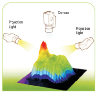
SPI utilizes angle cameras that take rapid 3D pictures to measure solder paste volume and alignment. The SPI software also provides key data about the printing process that helps identify whether any defects are caused by the solder or by another source which can then be corrected early in the assembly process.
Because SPI rapidly identifies any imperfect solder volume or alignment process variations, SPI significantly improves print quality and yield—assuring the efficient production of high quality, high performing PCBs while controlling costs due to rework.
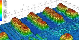
SPI has undergone its own evolution from 2D to 3D capability. 3D captures the height of the solder paste printed (also known as the "Z", for Z axis), which enable the equipment to more accurately measure total volume of paste printed. The 3D SPI, together with Automated Optical Inspection, enables contract manufacturers to adequately control and monitor both the solder paste printing process and component placement process.
Manufacturers who are serious about managing delivery time, cost containment, and zero defects, therefore, rely on 3D SPI to ensure that the solder print process functions within acceptable tolerances, producing the highest quality PCBs available.
Our blog, What Is “World Class” for Solder Joint DPMO? describes the fact that high-value contract manufacturers aim for Six Sigma quality for solder joints in surface mount technology. SPI is a critical part of that lean assembly process and, together with Automated Optical Inspection, plays a significant role in quality control and in customer satisfaction.


